Monday, November 5, 2012

Optical Components of an Optical Mouse (with real photos of mouse internals)

The working of an optical mouse can be divided into 2 broad areas -
  1. The OPTICAL part (discussed in this post)
  1. The ELECTRONICS (DIGITAL SIGNAL PROCESSING) part (not discussed in this post)


This post completely describes the optical aspect of the optical mouse (only). The electronics aspect is not discussed here.


Intended Audience -
This post is intended for those having elementary optics knowledge. If you wish to revise your preliminary optics knowledge, you can go through the beginning of these weblinks - refraction, total internal reflectionconvex lens.

Working of an optical mouse[in brief] -
At the bottom of your mouse, you can see a red light (or sometimes blue or no light, meaning infrared)  When you move the mouse, this light strikes the bottom surface on which the mouse is moving, gets reflected back and falls on the another part of the mouse, where a lens collects all the light and focuses it on a sensor with a DSP chip. This chip handles the computational aspect of the mouse working where it decides, depending upon the light falling on it, the direction in which the mouse moved and accordingly sends the signals to the computer. The optical components of the mouse are discussed below in greater detail.


Mouse Internals -
The mouse internals have been shown pictorially, for easy understanding.

On removing the top cover of the mouse. Visible components are labelled.


Separating the electrical (top part) and the optical (bottom part) components, with the inverted view of the electrical component. The tiny camera converts light falling on it into electrical signals for further processing.

Separating the electrical (top part) and the optical (bottom part) components. The optical component is just the transparent part, placed on the bottom (orange) support.

The system consists of 2 simple optical components. Their side view is shown. 

Front view of optical component #1

Optical Component #1: The complete blue highlighted part is the light transmitter. (There is a schematic below which can help in visualizing it better). It consists of a half convex lens/part and a long tunnel to carry light rays via TIR (Total Internal Reflection). The convex part above is to increase the field of view ie to take in more light without loosing them out due to non TIR ie to the make critical angle effectively smaller 

Top view of optical component #2
Optical Component #2: It is a simple convex lens, for magnifying the contents below it.

The small 42sec video below shows the 2 components from various angles. Note its size, as compared to my fingers.


Schematic and working of Optical System -

I have shown how the real optical components look like above. Here is a schematic of the same, from the side view -


Assume points P and U are on a rough surface, hence not getting reflected at same angles.


Optical Working:
Component #1 has 2 subcomponents -
The convex lens of component #1 (bulge), which collects light from a large solid angle and passes it to 2. The transmitter of component #1 (slanted rectangular part), which transmits light received at input to its output using total internal reflection. Component #1 thus illuminates the surface on which the optical mouse is moved.

Component #2 is a simple convex lens which focuses the illuminated surface below on the camera pin hole above, from .

Experiment -
I performed a simple experiment to understand (and verify) the working of the optical component. The aim was to try to read,  using the optical component, the alphabets "A B C D E F G H" written on the paper in a small font. (See pic below).


The (transparent) optical system (along with its orange support) is moved on the paper which has handwritten letters "A B C D E F G H", just like we move the mouse on a plain surface.


Observation & Conclusion -
Observation: After illumination and magnification, the letters could easily be read using the optical component.
Conclusion: The optical aspect involved in an optical mouse is theoretically quite simple.

The aftermath:
The DSP takes successive photos of the surface below & using the difference in successive images, figures out the direction in which the mouse moved. More information can be found on Wikipedia.

--------------------------------------------------------------------------------------------------------------------------

In one of my advanced optics course (EPL445) at IITD, we were asked to give a small presentation on some optical system, stressing on the optical aspect of it. While most students gave presentations on complex optical systems, none were a complete explanation since they were too complex to be clearly explained in  a short duration of 30 minutes. So, I decided to present on this topic (which was actually very simple considering the level of the course) in the interest of time. 

Sunday, January 1, 2012

Simple calculator display logic circuit (made using logisim)

The circuit consists of a 12 digit decimal display where you can insert numbers by pressing buttons 0-9, clear a recent number using the backspace button or clear all digits using the clear all button, just like we observe on a handheld calculator device. I have explained how I made the logic circuit in this post.

Below is a video of how the logisim circuit looks like and how it works. (Alternatively, a high quality picture (~24 megapixels) of the complete circuit together can be found here.) You can also try running/simulating the circuit in logisim yourself by downloading the logisim circuit file here.


Intended Audience -
This post is intended for those having elementary digital electronics knowledge (mainly logic gates and flip-flops). Prior knowledge of logisim software will be useful. (If you are new to logisim, you can find some tutorials here. It is very easy to understand.)

This is a simple, non-timed circuit and hence it is not necessary to program this on verilog/VHDL. Also, note that this might not be the way how the circuit is implemented practically on devices like handheld calculators, mobile phones, etc. But, this circuit will surely work if implemented.

Calculator Display -
The display part of the circuit looks as shown below. You can interact with the buttons (only).

Note the labels 0,1, ..., 11, n0,n1, ..., n11, Clear All, Backspace.
They will be used throughout the post for discussing the circuit.
[In logisim, they are the Tunnel elements, part of the Wiring library]


The circuit consists of 3 important subcircuits - 

1. Taking input from buttons -
We need to store the value of the button when it is pressed. Note that pressing a button means logical 1 for a moment only; the button is not held continuously at logical 1 position.

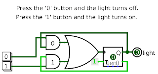
Directly understanding the circuit required for taking decimal input can be a bit confusing. Hence, it would be better to first understand the basic circuit required for taking a boolean input from the circuit below -

Since we have a decimal display and not a boolean display, we won't use this circuit as it is. 

I have used the BCD representation (ie 0 -> 0000, 1 -> 0001, 2 -> 0010, ..., 8 -> 1000, 9 -> 1001) and so four bits are required to store one decimal value. So, we will require 4 similar subcircuits with slight modifications. Also, the output of each of these circuits will be connected to 12 bit shift registers, which corresponds to the display part of the circuit. (This is discussed in the later part "Bringing together the subcircuits".) The shift registers are discussed next.

2. Shifting the input - 
As buttons 0-9 are pressed, existing input should shift to accomodate new digits. Similarly, when backspace is pressed, the newest digit should be discarded and the entire remaining input should shift back one place. Thus, input needs to be shifted in both left and right directions.
    Thus, we need a left right shift register. Since, our display is 12 digits wide, our left right shift registers should be 12 bits wide and we would need 4 such shift registers (for the BCD representation).

This is the circuit of a classic 4 bit left right shift register (rem. we need "12" bit shift registers) -

4 bit left right shift register (click to view full size image)
Symbol for 4 bit l/r shift reg. subcircuit
(It is used in the next subcircuit below)

Using 3 such 4 bit shift registers, we can make a 12 bit shift register as shown in the below circuit.

 
12 bit left right shift register (click to view full size image)
 
Symbol for 12 bit l/r shift reg. subcircuit
(It is used in a subcircuit below)

Note that, in the above circuit, I have kept the value of Data in left shift as 0 because when backspace is pressed, we wish to insert 0's from the other end (the most significant digit's end). Also, we don't need the Data out Left Shift, as it is to be discarded! And Data out Right Shift won't be required, as the circuit is designed such that one cannot push in more digits once the display is full, so no data will ever come out on right shifting at any point of time.

3. The clock
The clock is an essential part of any digital circuit which has memory. In this case the clock would be controlled by the buttons. When a button is pressed and held, it goes from logical 0 to logical 1 state and when it is released it goes from logical 1 to logical 0 state. These can be used as the rising and the falling edges of the clock respectively.

(Note: The label of the 12th bit is "11" because I have numbered the display bits starting from 0.)
(click to view full size image)

    When the display is full (ie the most significant digit, the 12th digit, is non-zero), we need to make sure that pressing buttons 0-9 should not bring in any more digits as there is no space left (just like it happens on a handheld calculator). Hence, we need an additional small OR gate (at the bottom of the above circuit). Note that backspace button should work no matter the display is full or not and hence it is directly connected to the clock. The backspace button also controls the LEFT_RIGHT parameter of the left-right shift registers. 
    Also, note that clear all means reseting all digits to 0 asynchronously. Hence, the clear all button does not come into picture here (ie it does not control the clock).


Bringing together the subcircuits -

1. Connecting the input taking circuit to the shift registers-
This is the most important part of the circuit. To store upto 12 digits, we need to connect the input taking subcircuit with the 12 bit shift registers. (We would need 4 such connections as shown below.) The most important trick here is to make the T flip flop rising clock edge triggered and shift registers falling clock edge triggered, otherwise the circuit won't work! (It took quite a lot of time for me to get this trick. Infact, I went on vacations before completing this circuit as I was stuck at this point for a long time!)

Labels bit0, bit1, bit2, bit3 correspond to the contents of the shift registers.

2. Making the display - 
There is nothing intelligent in this part. From the above subcircuit, we need to pull off 4 bits, 1 at a time from each shift register's contents (to make 1 unit of the 12 digit display), 12 times. If you don't understand this part, you can just ignore it here and try understanding it yourself by downloading the logisim circuit file (here) and playing with the circuit elements.

The labels 0,1,2, ..., 11 correspond to the 12 units of the display.
You must have seen these labels in the first picture in this post above.

The subcircuit for the clock is to be kept as it is.
A high quality picture (~24 megapixels) of the complete circuit together can be found here
You can also try running/simulating the circuit yourself by downloading the logisim circuit file here.

____________________________________________________

    I have not copied any part of this circuit from anywhere - either web or books (except the Shift Registers, but that is a standard circuit.). I made this logic circuit all by myself just out of pure interest and fun! I started making the circuit in the first week of December 2011, after I completed my 5th semester at IITD in which I learnt the basics of digital electronics (course EEL201). After making the basic subcircuits, I got stuck at the part where the input taking subcircuit had to be clubbed with the shift registers. (I was keeping both the T flip flop and shift registers as falling edge triggered.) After thinking for about 2 days on it, I left the circuit incomplete, afraid that I would have to restructure the entire circuit again, and went on vacations. After 2 weeks, I took a casual look at the circuit and to my surprise, within 10 minutes, found the solution! It was such a simple trick! But the most important one! (The trick was just to make the T flip flop as rising edge triggered, keeping the shift registers as falling edge triggered!) I was really happy that day as I didn't had to alter even a slightest bit of the circuit structure to make it working!  
    I realized that small changes can actually solve big problems in our lives, if we are not reluctant to try.